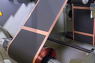
Inspection is a critical step in manufacturing, ensuring consistent product quality throughout the production process. Surface and visual inspections are typically performed using area cameras or line scan cameras, while some industries still rely on manual visual inspection. In recent years, however, inspection systems based on CIS line scan cameras have gained significant traction, offering an increasingly popular alternative for these applications.
Inspection systems using area cameras or conventional line scan cameras typically require a substantial working distance to deliver both high resolution and a wide field of view. In space-constrained production environments, meeting these installation requirements can be difficult.
CIS line scan cameras overcome these challenges by enabling high-precision inspection in a significantly more compact form factor, making them well suited for applications where installation space is limited.
High-Precision, Space-Saving Semiconductor Surface Inspection with CIS Line Scan Cameras
The following examples demonstrate how CIS line scan cameras are successfully deployed in semiconductor inspection applications, delivering high-performance imaging in space-constrained environments.
Compact Solution for Wafer Edge Inspection
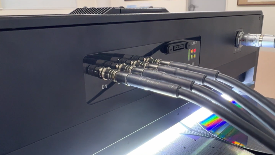
A semiconductor manufacturer required an inspection system for wafer edge inspection, but limited installation space made it impossible to accommodate a conventional camera setup. To overcome this challenge, a customized configuration that separates the sensor unit from the digital processing box has been developped, enabling seamless integration within the available space while maintaining inspection performance.
High-Speed Wafer Surface Inspection
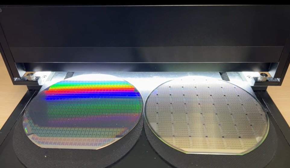
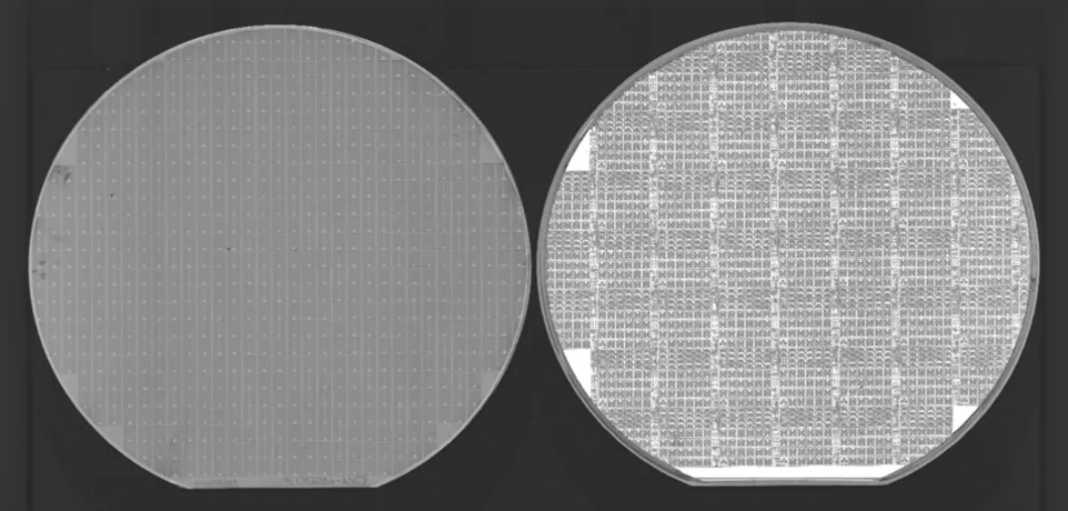
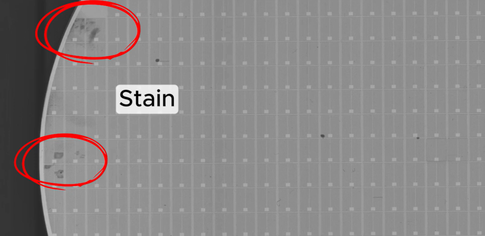
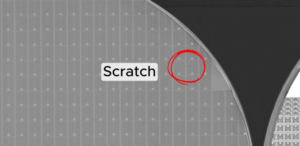
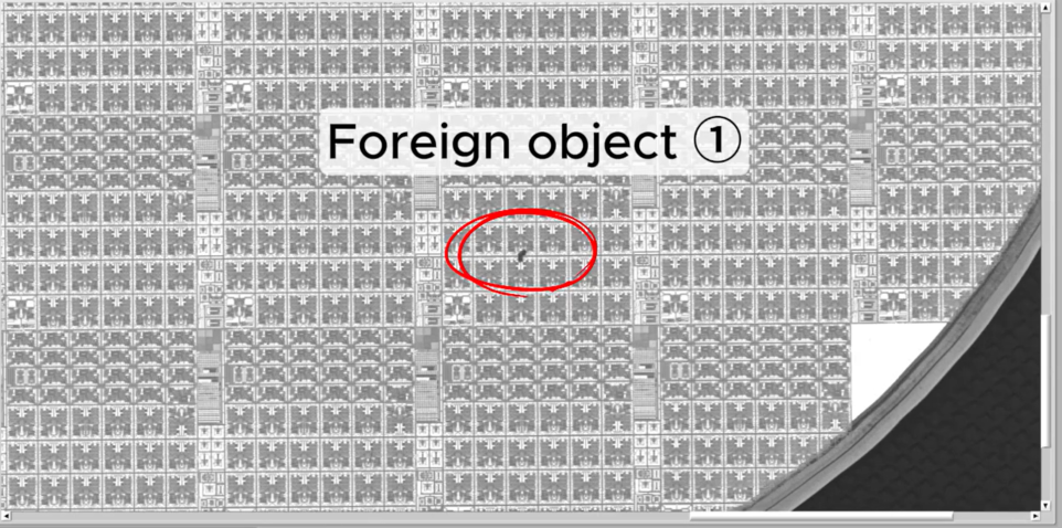
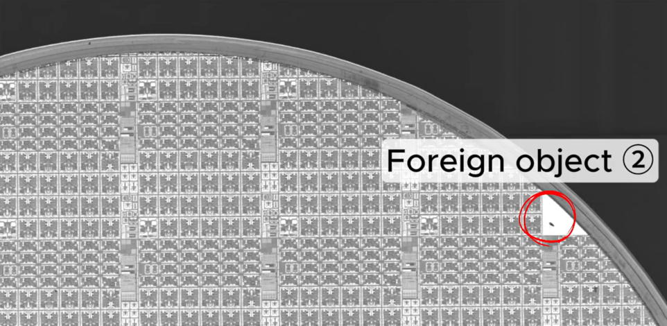
Another application involves detecting surface scratches and contamination on semiconductor wafers. In addition to the restricted installation space, the system required both high-resolution imaging and high-speed scanning.
To meet these demanding requirements, a solution featuring a separated sensor and digital processing unit has been implemented, combined with a CIS line scan camera offering 2400 dpi resolution (approximately 21 μm) and a CoaXPress 2.0 interface. This configuration deliveres the speed, image quality, and installation flexibility needed for a reliable inspection.
Optimized for Semiconductor Manufacturing
Both inspection systems use a special type of illumination technology, designed to minimize diffuse reflections from wafer surfaces and improve defect detection accuracy. In addition, fanless cooling CIS line scan cameras can be selected for both installations, eliminating airflow that could introduce particles into the cleanroom environment, a critical requirement for semiconductor manufacturing.
Expanding Semiconductor Inspection Applications
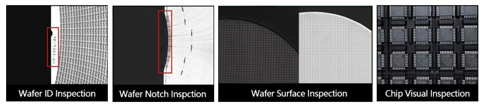
Beyond these examples, CIS line scan cameras are widely used across a variety of semiconductor inspection processes, including:
- Wafer ID inspection
- Wafer notch inspection
- Wafer surface inspection
- Chip appearance inspection
Their compact form factor, high resolution, and high-speed performance make CIS line scan cameras an ideal solution for modern semiconductor inspection systems where both accuracy and space efficiency are essential.